Starting in the Fall of 2017, the Physics Department will be offering a new major in Materials Physics.
Materials Physics majors will follow a curriculum that includes Condensed Matter Physics, Materials Synthesis and Applications, and Materials Characterization courses. This major is intended to prepare students to attend graduate school focusing on experimental condensed matter physics, materials science and engineering, and would be welcome in other interdisciplinary science departments. The students can work in science-related jobs in industrial settings, including engineering, teaching, and technical management.
The National Research Council has identified the national need to educate the next generation of scientists in particular researchers that grow high quality crystalline materials in the USA. Due to educational programs such as this major the experimental condensed matter physics community can continue to rely on high quality samples to answer important physics questions. Maybe more importantly materials discovery and characterization are critical for our ability to discover new materials for novel technologies and improve upon the existing ones. Students graduating with this new major will form the basis of this materials workforce of tomorrow.
Students in this major will be acquainted with topics covering materials synthesis, characterization and measurement. Examples of specific topics are,
Materials synthesis techniques:
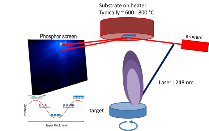
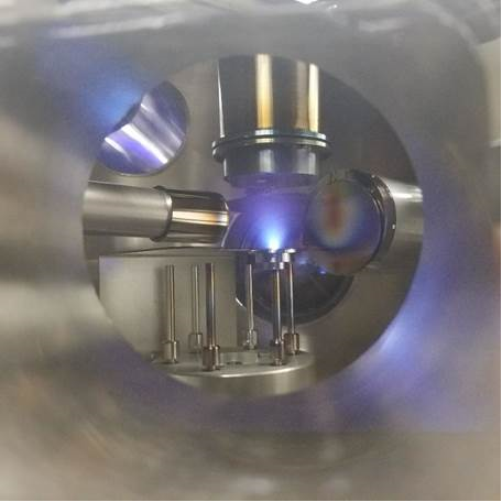
Example: Pulsed Laser Deposition, a technique in which a high energy laser is focused on a stoichiometric pressed pellet of material. This generates a plasma plume (see photo) directed at a substrate held at constant high temperature. Reflection high energy electron diffraction performed in-situ during growth provides information on the film thickness, roughness and surface symmetry of the crystal.
Materials Characterization:
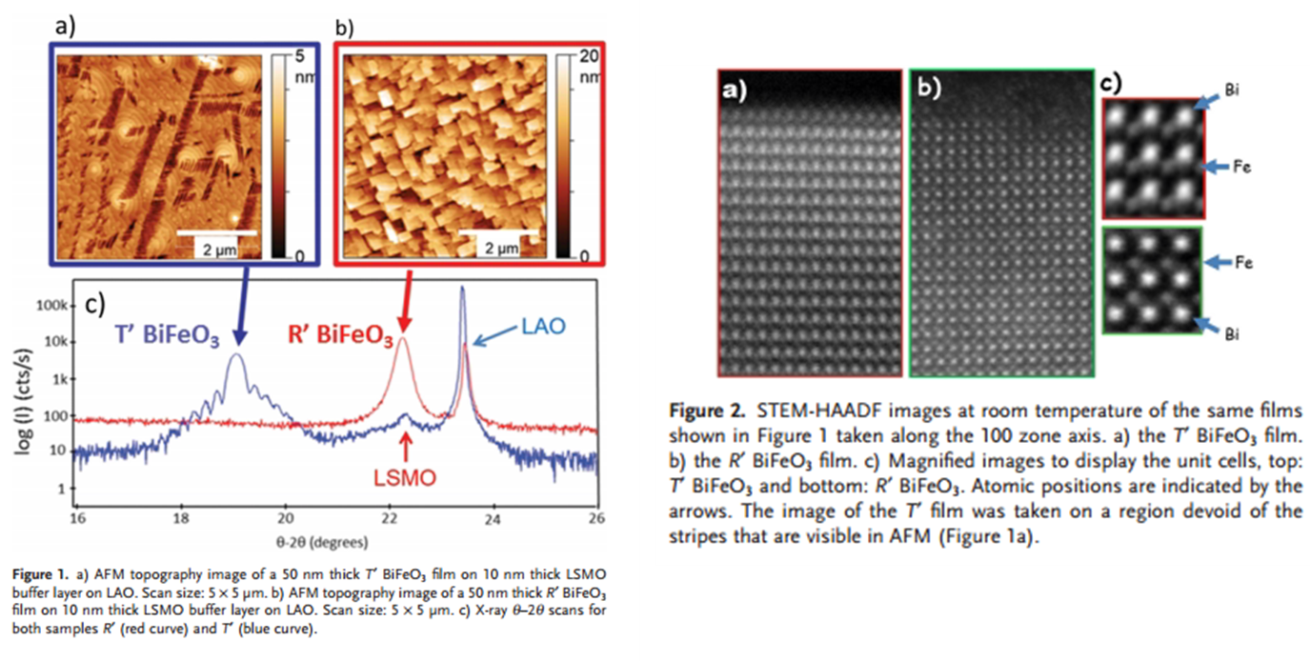
Various techniques are used for materials characterization; examples are x-ray diffraction, which allows study of the lattice structure (the precise atomic arrangement) within a material. Another example is atomic force microscopy (AFM) with which the roughness of the material surface can be investigated with nanometer scale resolution (Fig. 1 shows AFM and x-ray diffraction of bismuth ferrite films). Lastly, transmission electron microscopy, in which the structure of the material down to the atomic lenghtscales can be determined (Fig. 2 shows the atomic arrangements of the films in Fig.1).